Diode and BJT mechanism
A two-terminal semiconductor that allows current to flow one way but not the other.
Insulator.
Electrons saturate the holes in P, leaving no differential for the electrons in N to jump towards. Meanwhile, the extra electrons in N flow back to the battery.
Conductor.
Electrons saturate N, push into the depletion region, then jump across to the holes in P, which then return to the battery.
A large positive current is allowed to flow from collector to emitter.
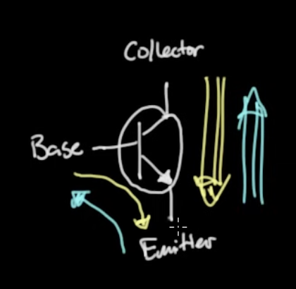
Image from Ben Eater's transistor video.
You're allowing electrons from the emitter to get all the way up into the base, so close that they can jump across the depletion region between base and collector.
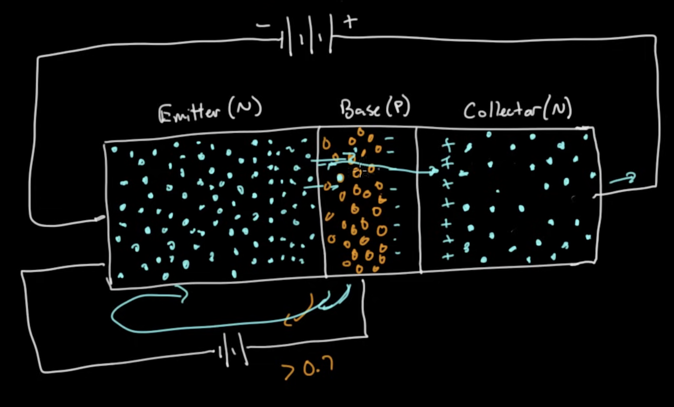
Image from Ben Eater's transistor video.
MOSFET vs BJT
Top to bottom: gate (metal) on top of an SiO₂ insulator, sitting on a P-type substrate. Two N-doped wells flank the gate on the left and right — the source and the drain. When the gate is positive, a channel of electrons forms in the substrate just under the insulator, connecting source to drain.
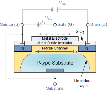
It pulls up the electrons in the P-type substrate, filling up the holes at the top — the channel.
In a MOSFET, the input is a voltage you set. In a BJT, it's a current you must keep feeding.
Thanks to the insulator between the gate and the channel, there's no power dissipated. The channel is powered just by voltage (basically potential energy).
When you turn the transistor on or off (i.e. when the gate voltage changes).
A capacitor.
Dennard scaling
As transistors shrink, their power density stays constant, so total power usage stays in proportion with chip area.
If you shrink both the voltage and the oxide thickness, the transistor keeps working the same way.
Since 1947
Its native oxide (GeO₂) is water-soluble and electrically defective. MOSFETs need a thin, stable, near-perfect insulator on the channel — only silicon grows one (SiO₂).
- Planar: gate sits flat atop the source-to-drain channel.
- FinFET: gate drapes the channel from three sides.
- Gate-all-around: gate fully wraps the channel from all sides.
Better gate control means you can shrink the source-to-drain distance (the "gate length") without source/drain fields leaking current through.