Diode and BJT mechanism
A two-terminal semiconductor that allows current to flow one way but not the other.
Insulator.
Electrons saturate the holes in P, leaving no differential for the electrons in N to jump towards. Meanwhile, the extra electrons in N flow back to the battery.
Conductor.
Electrons saturate N, push into the depletion region, then jump across to the holes in P, which then return to the battery.
A large positive current is allowed to flow from collector to emitter.
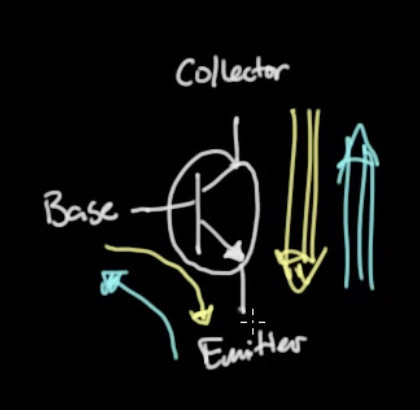
Image from Ben Eater's transistor video.
You're allowing electrons from the emitter to get all the way up into the base, so close that they can jump across the depletion region between base and collector.
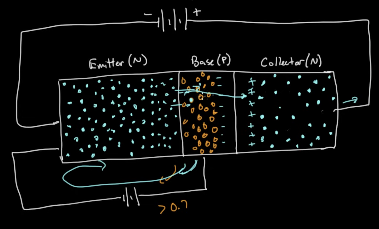
Image from Ben Eater's transistor video.
MOSFET vs BJT
Top to bottom: gate (metal) on top of an SiO₂ insulator, sitting on a P-type substrate. Two N-doped wells flank the gate on the left and right — the source and the drain. When the gate is positive, a channel of electrons forms in the substrate just under the insulator, connecting source to drain.
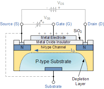
It pulls up the electrons in the P-type substrate, filling up the holes at the top — the channel.
In a MOSFET, the input is a voltage you set. In a BJT, it's a current you must keep feeding.
Thanks to the insulator between the gate and the channel, there's no power dissipated. The channel is powered just by voltage (basically potential energy).
When you turn the transistor on or off (i.e. when the gate voltage changes).
A capacitor.
Since 1947
Its native oxide (GeO₂) is water-soluble and electrically defective. MOSFETs need a thin, stable, near-perfect insulator on the channel — only silicon grows one (SiO₂).
Dennard scaling refers to the period from 1960-2005 in which planar MOSFETs were scaled down by directly shrinking their dimensions, which increased power density.
However, threshold voltage and leakage current do not scale with transistor length - Source and Drain got so close together that they would be current even without the channel being on.
- Planar: gate sits flat atop the source-to-drain channel.
- FinFET: gate drapes the channel from three sides.
- Gate-all-around: gate fully wraps the channel from all sides.
Better gate control means you can shrink the source-to-drain distance (the "gate length") without source/drain fields leaking current through.
Gates and arithmetic
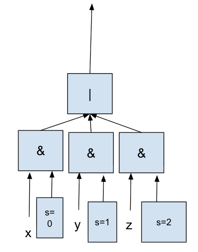
Selection — a ternary operator for two inputs.
A full adder considers the carry-in; a half adder doesn't.
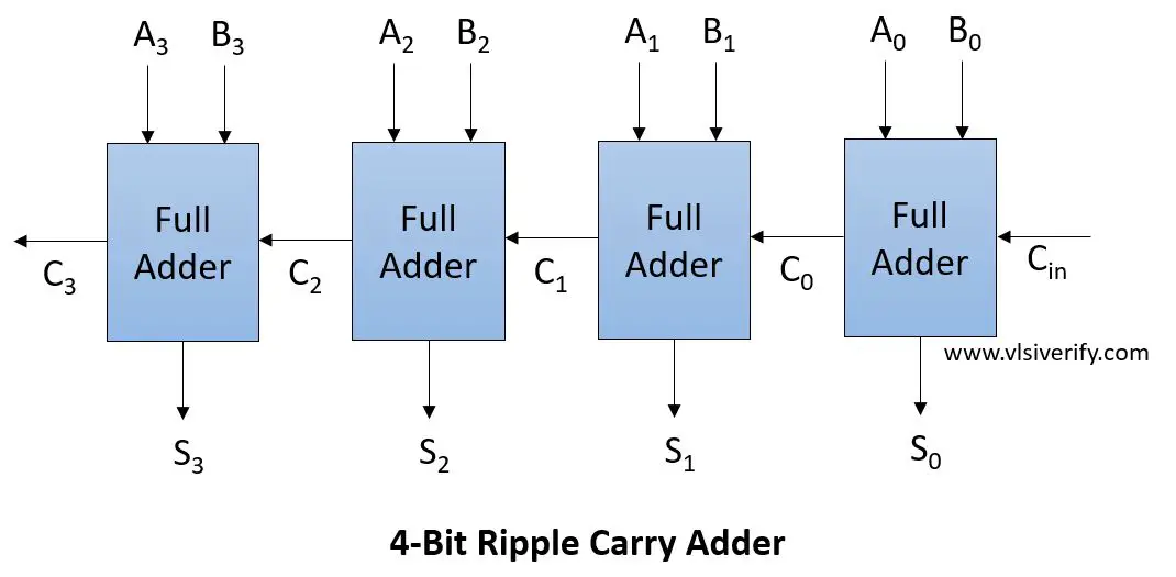
A horizontal chain of 4 full adders. Each takes a pair of bits plus the previous adder's carry-out as its carry-in, and emits a sum bit plus a carry-out that feeds the next adder.
Consider the simpler 4×4 case: (with the accumulate).
This breaks down into
Each of those is in turn a mux:
So you need as many adds and muxes as there are digits in the first number.
The width of both gates has to be twice the width of the biggest number, since an 8-bit × 8-bit product can be 16 bits wide.
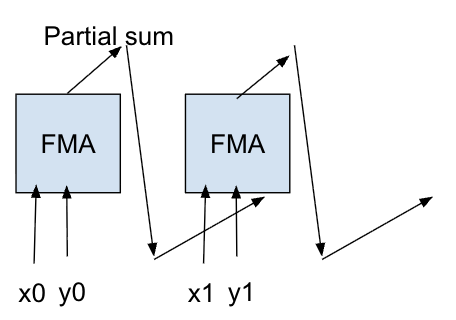
For two length- vectors, run sequential FMAs: for . The accumulator ends up holding .
RTL to GDS, clock speed, memory
- Logic synthesis: compile RTL → technology-independent graph of universal gates (NAND-ish).
- Technology mapping: collapse the graph by pattern-matching the larger patterns of TSMC's standard cell library onto it ("regex for trees") → technology-dependent netlist.
- Placement: embed cells in 2D minimizing wire length (spring / cost-function optimization).
- Routing: connect placed cells with wires on stacked copper layers (Manhattan-only).
- GDS-out: lower placement + routing to polygons (doping, etch, metal) → mask data for TSMC.
Clock speed is set by the critical path — the longest delay between any two registers (wire plus logic cost). Two chips on the same node can have a different layout, affecting this quantity.
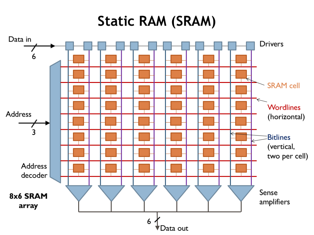
SRAM is much smaller per bit but rigid (1R xor 1W per cycle); register files are bigger per bit but flexible (cheap to add ports, no minimum size).
Because of how it's implemented: an SRAM is a hand-designed macro with exactly one decoder + one set of bit lines wired into the grid.
Fabrication
In thermal oxidation, you're actually reacting with the silicon directly to make a new compound (Si -> SiO2) whereas in chemical vapor deposition, you're reacting some precursor gas to accumulate atop the existing material, not by turning it into something
Without the nitride atop to prevent thermal oxidation atop the corners of the trench, you'd create bonds there which are bent. Even once you mechanically polish them atop, they'd be vulnerable to mechanical stress, but with nitride atop they form clean molecular structures.
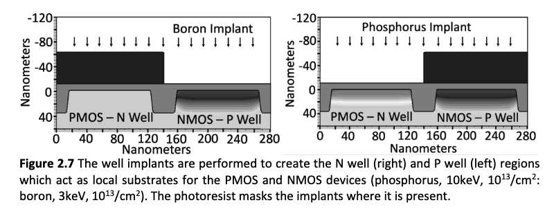
As the NA (the concentration angle) of the lithography increases, you have to use thinner layers of photoresist, lest you have inward sloping edges because of light angle. Thin resist can't block high energy well implants.
As transistors got smaller, silicon dioxide would let too much current leak between the gate and the channel. High K metal gates have better capacitance.
The gate consists of several metals that are chosen to optimize the conductivity of the gate and threshold voltage of the device. They can melt and degrade when subjected to high temperature processes that occur at the beginning of transistor fabrication. Therefore, they are deposited last to avoid these high temperature steps.
The first precursor gas is passed over the wafer. It typically has a metal part and an organic part. The metal portion binds to the surface, forming a single layer with the organic sticking up. This process is self-limiting because binding only happens between the wafer and the metal, not between the metal and the organic. Next, the chamber is purged and the second precursor is introduced. This gas reacts with the dangling organics pulling off the organic part of the molecule and leaving a single atomic layer of the metal. This process is repeated for as many layers as desired.
Interconnects and lithography
Copper diffuses so much that if it was directly touching the transistor, you'd worry about it damaging sensitive areas. So we used Tungsten there.
Tungsten has higher resistivity, so it would require more power for all the interconnects if we used tungsten all over.
Ruthenium is easier to etch than copper, which allows you to etch out air gaps (air has the lowest capacitance)
At nanoscale, ruthenium has lower resistance, because mean free path of an electron is lower, which means it accumulates and thus dissipates less energy between collisions
DUV masks are transmitting, meaning they selectively transmit or absorb light based on the pattern. Since every material absorbs EUV light, this approach cannot be used in the EUV case. Instead of transmitting, EUV masks must be reflective in the regions where the resist should be exposed.
1. EUV masks are reflective, so the blank mask must be made of 40-50 alternating layers of silicon and molybdenum. This structure is hard to fabricate. 2. Patterning the mask requires a dedicated multi-beam electron lithography tool. Inspecting the mask for defects requires another dedicated high-resolution inspection tool. Mask yield is ~50% which increases cost. 3. To keep dust particles off the mask, a pellicle must be placed over the mask which must be ultra thin and temperature resilient.
1. As the NA increases, the lenses become very large. Large lenses mean that the light will strike the lenses at a large angle. At large angles different polarizations of light are reflected differently. This reduces the contrast between the absorbing and reflecting parts of the mask. 2. The depth of field (DOF) quantifies what thickness of the resist is in focus during exposure. DOF ~ 1 / NA². Therefore, as the NA is increased, the DOF gets smaller, meaning a thinner resist must be used. Thinner resists are worse at blocking subsequent etching steps.