Gates and arithmetic
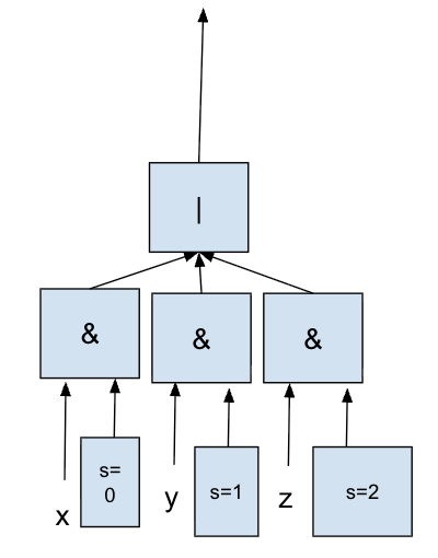
Selection — a ternary operator for two inputs.
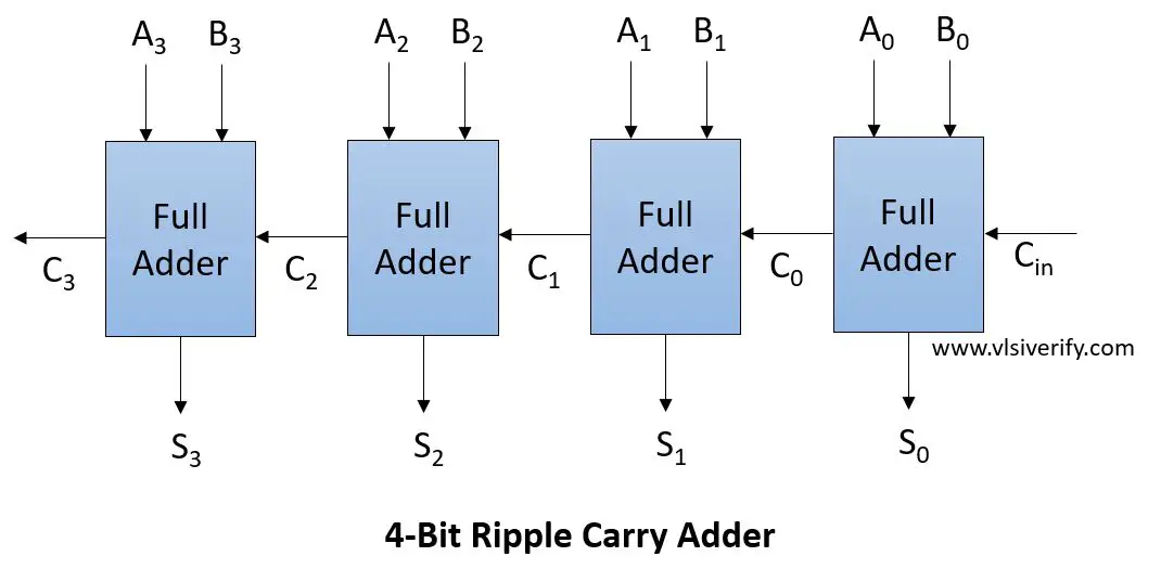
A full adder considers the carry-in; a half adder doesn't.
A horizontal chain of 4 full adders. Each takes a pair of bits plus the previous adder's carry-out as its carry-in, and emits a sum bit plus a carry-out that feeds the next adder.
Consider the simpler 4×4 case: (with the accumulate).
This breaks down into
Each of those is in turn a mux:
So you need as many adds and muxes as there are digits in the first number.
The width of both gates has to be twice the width of the biggest number, since an 8-bit × 8-bit product can be 16 bits wide.
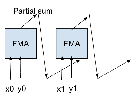
For two length- vectors, run sequential FMAs: for . The accumulator ends up holding .
RTL to GDS, clock speed, memory
- Logic synthesis: compile RTL → technology-independent graph of universal gates (NAND-ish).
- Technology mapping: collapse the graph by pattern-matching the larger patterns of TSMC's standard cell library onto it ("regex for trees") → technology-dependent netlist.
- Placement: embed cells in 2D minimizing wire length (spring / cost-function optimization).
- Routing: connect placed cells with wires on stacked copper layers (Manhattan-only).
- GDS-out: lower placement + routing to polygons (doping, etch, metal) → mask data for TSMC.
Clock speed is set by the critical path — the longest delay between any two registers (wire plus logic cost). Two chips on the same node can have a different layout, affecting this quantity.
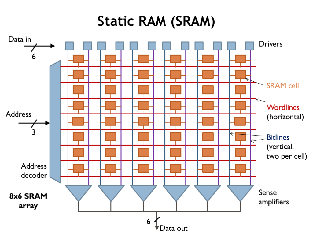
SRAM is much smaller per bit but rigid (1R xor 1W per cycle); register files are bigger per bit but flexible (cheap to add ports, no minimum size).
Because of how it's implemented: an SRAM is a hand-designed macro with exactly one decoder + one set of bit lines wired into the grid.